1.High speed 6S inspection solution for chip sorting. 2.Switchable flip function for face down/up application. 3.Large die size range(0.5-50mm) inspection. 4.Flexible load/unload system option for waffle pack/JEDEC tray/tape reel 5.Die thickness measurement optional.
1.Accuracy:X,Y= ± 30μm , θ=± 0.2° 2.Cycle Time:≦ 0.3 sec/chip (exclude process time) 3.Chip size:0.5mm~ 20 mm (option: ~2 x 50mm or customized) 4.Die Thickness:0.10 mm~2 mm (2mil Option) 5.Pick up force: 50~150g 6.Wafer Size:12” Standard (8” Option) 7.Input Load/Unload : Automatic 8. Tray size:2”,3”,4” 9.Output Load/Unload : Automatic 10.Binning Capability :3 bins(Option 6 bins) 11.Topside /Backside insp.:Chipping, Crack, Residue glue , defect size>10um 12.Side wall inspection:Chipping, Crack, defect size>10um 13.Mapping:Easy mapping/File mapping/Barcode auto loading
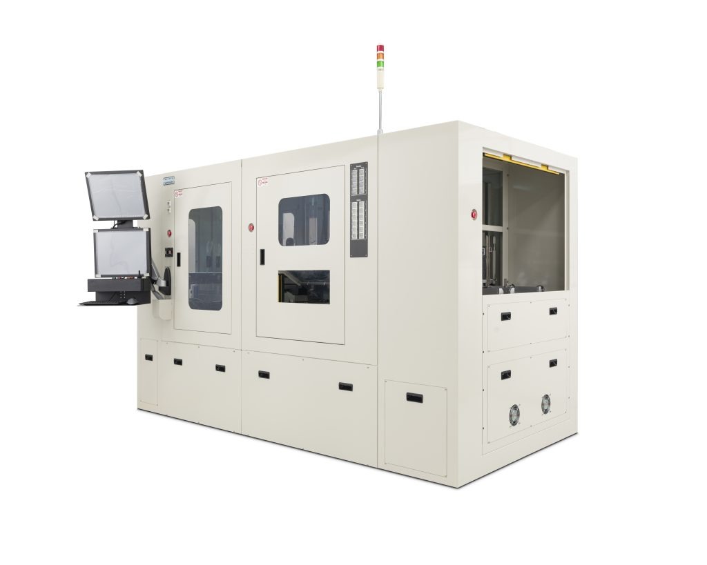
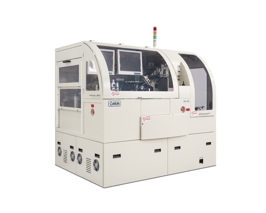
KS-812
KS-812
1.Quick and easy change among 2, 3, 4-inch trays. 2.Dual feeder for continuous tray operation. 3.High speed and reliable linear Pick & Place module. 4.Particle-proof design for tray transfer system. 5.Real time chip backside inspection in P&P process (option function) . 6.Automatic bin sorting system for 3 or 6 bins of chips. 7.Wafer mapping function available.
1.Automatic bin sorting system for single bin & multi bin. 2.Quickly change tape frame design. 3.Output Feeder stage for 8² and 12² is changeable. 4.Wafer mapping function is available. 5.Wafer /Carrier available, kit exchange easily. 6.High speed and reliable linear Pick & Place module.
1.Accuracy : X,Y=±50μm,θ=±0.2° 2.Cycle Time : ≤0.5 sec(Excluding pick and place delay time) 3.chip size : 0.6×0.6mm~25x25mm 4.Die thickness :0.2mm~0.7mm 6.Wafer Size : >12″ Standard(8″ Option) 7.Input Load/Unload : Automatic 8.Output Load/Unload : Automatic 9.Binning Capability : Single bin/Multi Bin 10.Flip funcition:Option 11.Mapping : Easy mapping/File mapping/Barcode reader(Option) 12.Tack Time(for wafer change at unloader) : ≤10 sec
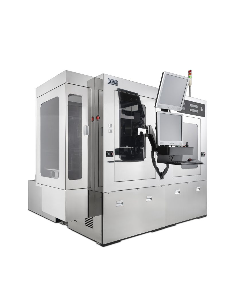
KS-956/962
KS-956/962
1.High Speed 6S inspection solution for chip sorting. 2.Side wall inspection:Chipping, Crack, defect size 30um. 3.NG die output:Place bad die(by inspection)on tray for rework or review. 4.Barcode reader:For mapping file confirming. 5.SECS:For mapping data transfer (option)
1.4-Heads pick & place module. 2.AOI & Die transfer parallel processing Preciser. 3.High speed 12-Heads rotary module. 4.Dual working tray table for quick exchange Take & supply trays in run state. 5.Pre-peeling module is available. 6.Quick wafer exchange module is available. 7.Heating ejector is available.